Levitating Magnet Project
Problem Definition
The following project required designing a controller to stabilize and levitate a permanent magnet. This
report also covers the hardware required for the actual implementation; however, we are only required to talk about each individual component and how it fits into the whole system. The objective is simply to
understand all the components required so that the physical implementation of the suspension system
can be completed next semester during the capstone.
How Circuit Works
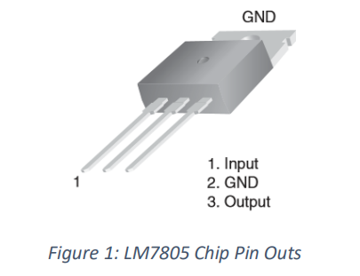
Terminal Regulator – LM7805
This IC chip is configured in the Fixed-Output Regulator configuration from the datasheet. The output
voltage is expected to be approximately 5V on a typical chip with the variation being approximately
±0.25V. The chip has three terminals the input, ground, and output. The chip has those pins in order
from left to right, as can be seen in figure (1).
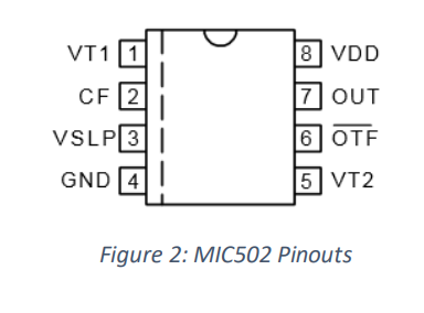
Fan Management PWM Controller – MIC502
The chip is responsible for producing a low-frequency pulse-width modulated (2) output for driving
external motors. The pin configuration is a figure (pin-out). Pin 1 and 5 are both used as inputs. Pin 2 sets
the frequency for the PWM output wave. Pins 3. Pin 4 is the ground for the chip. Pin 6 indicates when
the temperature passes a threshold. Pin 7 is the output of the chip, which provides the PWM waveform
that is generated from the highest value between pin 1 and pin 5. Pin 8 is where the voltage supplied
from the power supplies goes.
TTL Inverter – 74LS04
The pinouts can be seen in Figure (3).
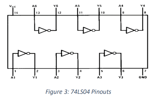
Pin 14 is responsible for the power supplies, and pin 7 is the ground. All the odd number pins are for the
inputs, and the odd values provide the outputs. For the Inverter, all the input values, which should be
either 0V or 5V provided the opposite values for the output. For instance, if the input is high, the
output is low, and vice versa. The supply is recommended to be at approximately 5V. For the input signal
should hit a threshold of 2V and for it to be considered low the input must go under 0.8V. When the
output voltage is low it will have a maximum value of 0.5V and typically hover around 0.35V, when the
output voltage is high it will have a minimum value of 2.7V and a typical value of 3.4V.
Bridge Motor Driver
The device has bidirectional drive currents up to 600 mA at voltages from 4.5V to 36V. This chip
requires the inputs to be transistor-to-transistor logic. Input to the H-bridge should be a signal that
switches from 3V to 0V, with the lowest high voltage accepted being 2.3V and the highest low voltage
is 1.5V. The output is a signal that switches from a Low voltage to a high voltage that is
representative of the low or high input voltage. The duty cycle of the input will determine the output
current at each of the outputs. If the duty cycle is at 50% there will be no output or input current coming
from or to the output pin.
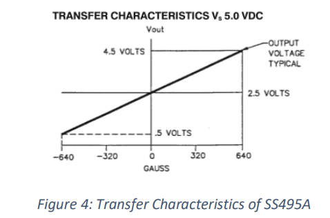
Hall Effect Sensor – SS495A
The supply voltage (Vs) to the chips is required to be within 4.5V to 10.5V. The magnetic range of the
sensor is typically from -670 to 670 Gauss. The output voltage is between 0.2V to 0.2V below Vs. As the
magnetic field increases to a positive value, the output voltage is increased to its maximum as well. The
output voltages also decrease as the magnetic field becomes more negative as seen in figure (4).
Entire System Description
In our case for the MIC502, pin 1 is the input that comes from the compensator. Pins 3 through 5 are set
to ground, with pin 5 continuously being compared to the input from the compensator. This is done so
that the PWM can be controlled completely by the compensator. Pin 7 is not connected because we do
not expect the circuit to experience overheating. The chip is powered from the output of the voltage
regular on pin 8, which is expected to be 5V. The PWM frequency is determined from the graph in
figure (5). Since we are using a 680pF, the frequency is above the 3KHz limit.

For the inverter, the PWM is coming out from the one inverter and driving the bottom part of the H-bridge. That inverted signal is also inverted again and sent to the input of the top part of the H-bridge.
The H-bridge will be responsible for generating the electric field in the coil. One side of the coils is
connected to an output from the PWM that was inverted once, and the other side of the coil is
connected to the output from the PWM that was inverted twice.
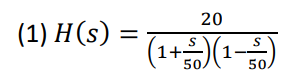
Theoretical Design of Controller
The plant, H(s), of the system (1) was provided with a pole on the left-hand plane (LHP), and another on
the right-hand plane (RHP).
The controller, A(s), was designed with the general form (2) in mind.

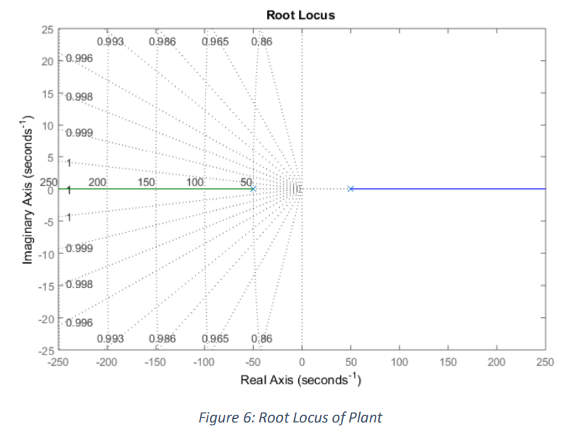
The negative sign comes from the fact that we are required to use an inverting operational amplifier (op
amp) to stabilize the system. Without the negative sign, the pole on the right-hand plane does not
converge to the left-hand side as the gain is increased. This can be seen on the root locus of the plant in
figure (6).
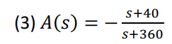
An arbitrary zero was chosen far enough from the imaginary axis to ensure the RHP pole crossed into
the LHP and the beta value was arbitrarily chosen far enough to ensure the overshoot was not too high.
These parameters lead to the creation of the controller (3), which can be alternatively be expressed as
(4) as required for this project.

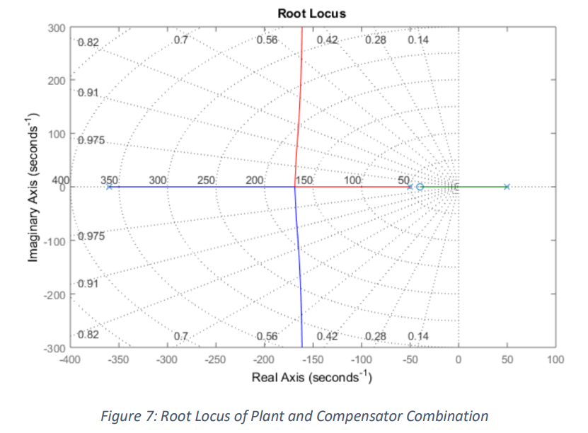
The gain on the controller was selected by combining H(s) with A(s) and finding the gain through the
root locus, as shown in figure (7), from the combination of the two.
Bode Plot of A(s)H(s)
The bode plot of the open loop system was generated using MATLAB and can be seen in figure (8).

Nyquist Plot of A(s)H(s)
The Nyquist plot was generated by combining the lead compensator, the plant, and the chosen gain for
the compensator.

The Nyquist plot is required to encircle the -1 point to make the system stable since it has an RHP. The
gain margin on the system is -6.94 dB, and the phase margin is 53.1 degrees. Which is slightly less than
the ideal of 60 degrees, but still provides stability to the system.
Root Locus of 1+A(s)H(s)
The root locus of this is used to view the poles of the closed loop system. When creating the closed loop
system 1+A(s)H(s) goes on the denominator. Therefore, the zeros on this root locus represent poles on
the actual closed loop. In the graph below, the zeros, which represent poles located at the position
of the gain of the closed loop system, are shown in figure (10).

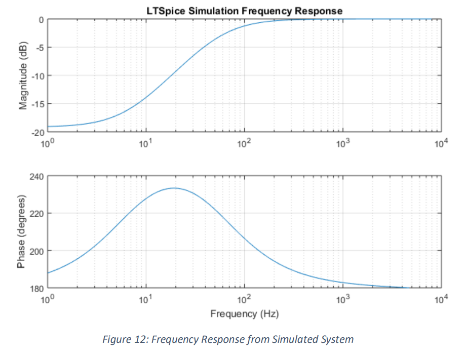
LT Spice Design
The design for the controller came from the transfer function established in (4). The series combination
of the resistor and capacitor at the input creates the zero, and the series combination at the feedback
creates the pole.
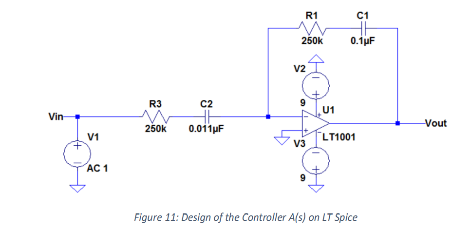
The bode plot was included in the report to highlight the similarities between the physical controller
in figure (LT Spice circuit) and the simulated transfer function on equation (controller) responsible for
the physical controller.
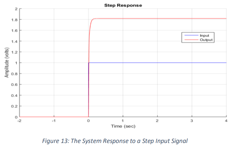
Unit Step Response
The closed loop system was used to get the step response of the system. The simulation was made by
putting a unit step at the input and obtaining the output. The output signal was shown to be stable with
a steady state error in figure (13).
Design of Digital Phase Lock Loop
Design of VCO
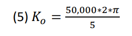
The frequency range is 25kHz to 75kHz. With an input of 0 to 5V. The value 𝐾𝑜 (5) is the gain from the
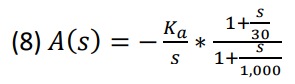
voltage-controlled oscillator (VCO), the 𝐾𝑑 gain (6) comes from the phase detector, and 𝐾𝑎 (7) is the gain
from the controller, A(s), shown in equation (8).


The values chosen for the capacitors and resistors that decide the frequencies generated by the VCO are
shown below in (9) through (11).

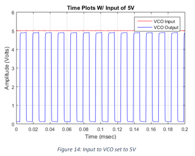
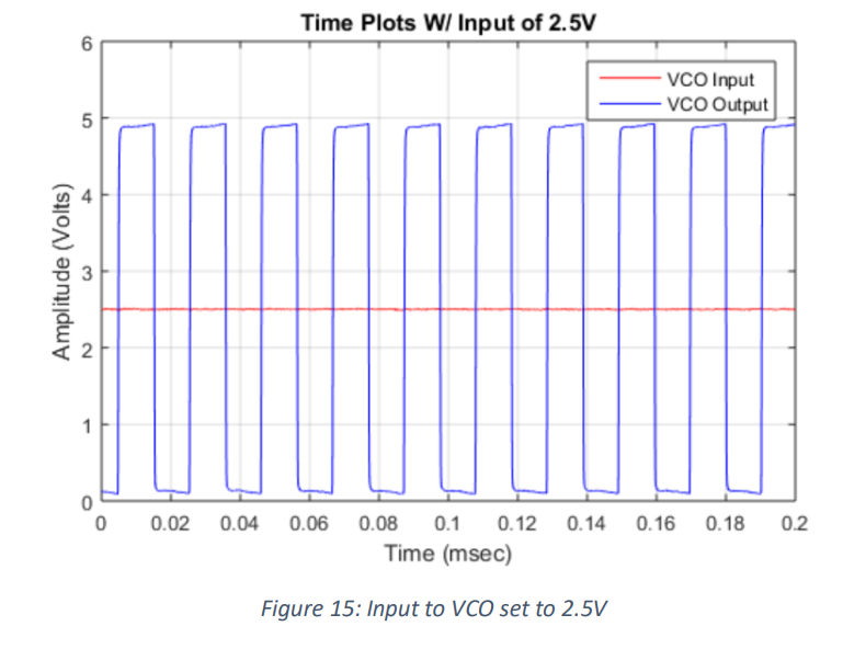
To test the ranges produced by the VCO, and to check if it worked, I decided to use a 0, 2.5, and 5 volts to
determine the different frequencies produced. At 5 volts, the maximum frequency produced by the VCO
was a 66.8kHz waveform shown in figure (14).
When the input voltage was set halfway the output showed a 48.1kHz waveform, as seen in figure (15).
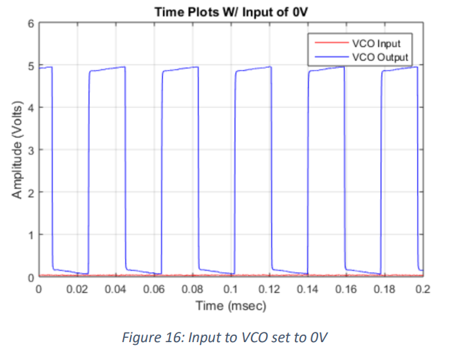
When the input voltage was set to the lowest point of 0V the output showed a 26.3kHz waveform, as
seen in figure (16).
Theoretical Loop Gain Bode Plot
The theoretical loop bode plot is shown below. The open loop system is defined in (12) with the gain
equations from the previous subsection.

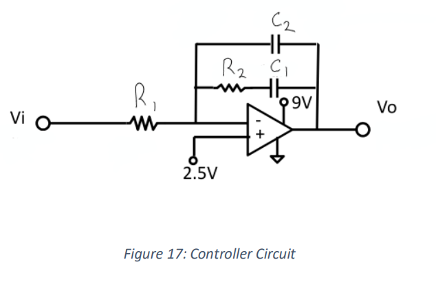
The transfer function derived from the controller, in figure (17), in terms of resistors and capacitors, is
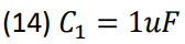
the following (13).
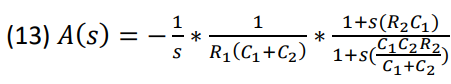
The component values used were found to be the following to meet the poles and zeros, (14) through
(17).

When the open-loop was plotted without gain I found how far above 0 dB the 100 Hz point was and
added the proper gain to make the loop bandwidth 100 Hz. The loop without the gain is below in figure
(18).
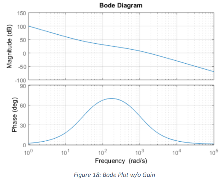
The gain was determined to be the following (18).
The new open loop, with the gain included, has a cross-over frequency of approximately 100 Hz as can
be seen in figure (19).

Build the circuit and display the input and output frequency
The input frequency was generated with a square wave that has a 50% duty cycle for the input of the
phase lock loop chip, I labeled it as the VCO input because it will be what the VCO will attempt to reach.
Both the input signal and the output of the VCO were displayed on the same plot to show how well the
system locks.
Input Frequency of 45kHz
When the input frequency was set to 45kHz the system attempted to track, but it would slowly drift
away, shown in figure (20).

Input Frequency of 55kHz
When the input frequency was changed to 55kHz the phase lock loop tracked reasonably well, as shown in
figure (21).