What is a Diode?
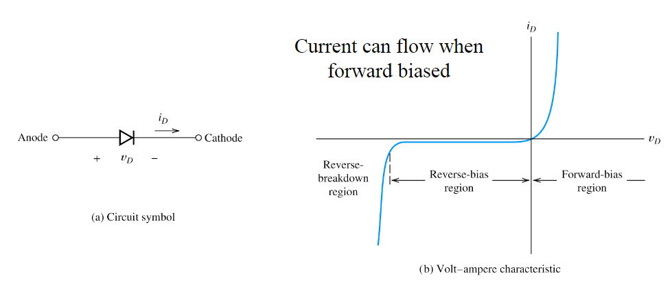
A diode is a semiconductor device that allows current to flow in one direction serving as a one-way current switch. Diodes, also called rectifiers, convert alternating current (AC) into pulsating direct current (DC). They are categorized by type, voltage, and current capacity. With polarity determined by an anode (positive) and cathode (negative), diodes typically conduct current only when a positive voltage is applied to the anode.
How does a diode stop current flow?
The current flowing through a diode is restricted to one direction, known as the forward direction. As a result, it blocks current attempting to flow in the reverse direction. Diodes can be likened to one-way valves in electronics. When the voltage across a diode is negative, no current can flow through it, making the ideal diode appear as an open circuit.
Are diodes still used?
Diodes are crucial in modern electronics despite their simplicity as two-pin semiconductor devices. They are widely used for converting AC to DC, isolating signals from a power supply, and blending signals together.
What is the IV relationship of a diode?
As indicated by the i-v curve, the current through a diode and the voltage across it are mutually dependent. Higher current results in higher voltage, while lower voltage leads to lower current. However, once the voltage reaches approximately the forward voltage rating, significant increases in current should result in only minimal increases in voltage.
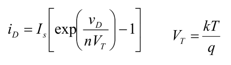
k = 1.38 × 10⁻²³ J/K is Boltzmann’s constant q = 1.60 × 10⁻¹⁹ C is the magnitude of the electrical charge of an electron. At room temperature. Is is the staturated current while Vt is the thermal voltage.
What is a simple diode circuit?
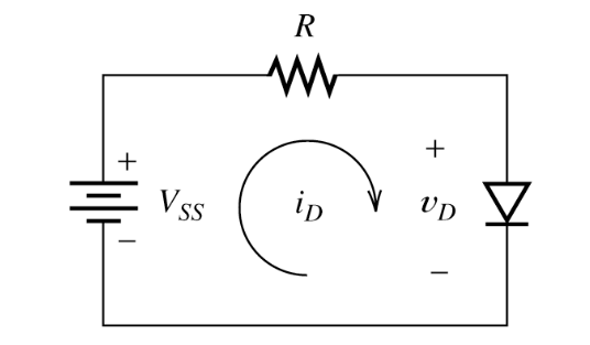
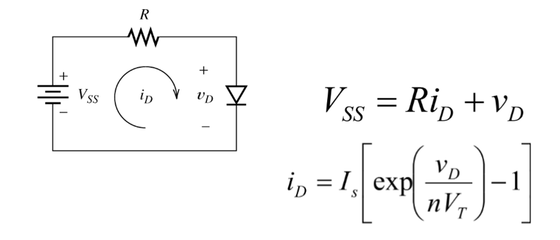
A basic diode circuit involves the use of a standard p-n junction diode to perform a specific function. In these circuits, a diode is commonly employed as a switch. Examples of such circuits include rectifiers, clippers, and clampers. The current iD will flow through R and the diode in the simple circuit below. There is a voltage drop on the diode.
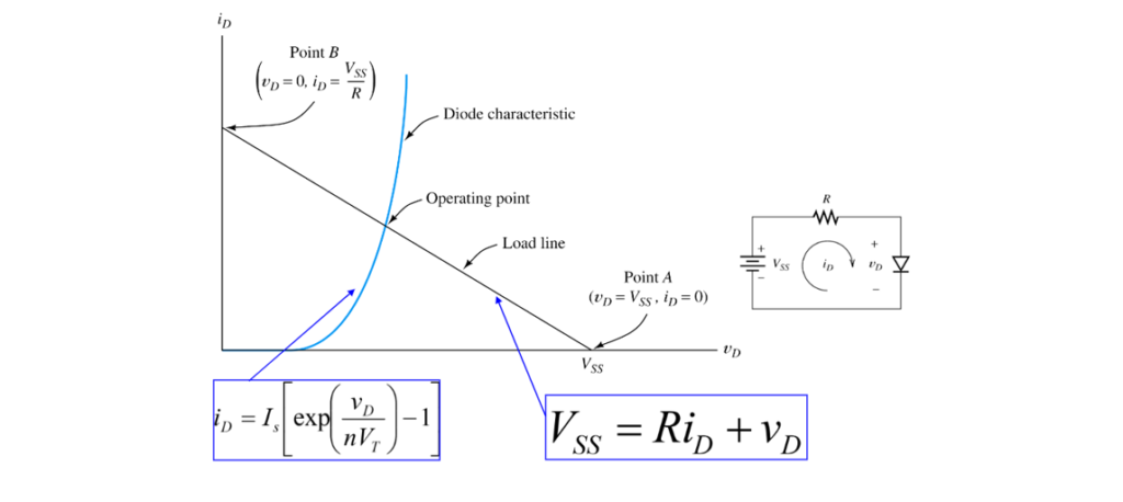
What is load line analysis of diode?
In the graphical analysis of nonlinear electronic circuits, a load line is a line that is plotted on the current-voltage characteristic graph of a nonlinear device, such as a diode or transistor. This line depicts the limitations imposed on the voltage and current of the nonlinear device by the external circuit. Using the simple circuit example above, Since vD is a function of iD, the above equation can not be solved.
Graphical analysis
To perform load line analysis, In the forward region, the current and voltage on each component satisfy an equation. Draw the line for each of them.
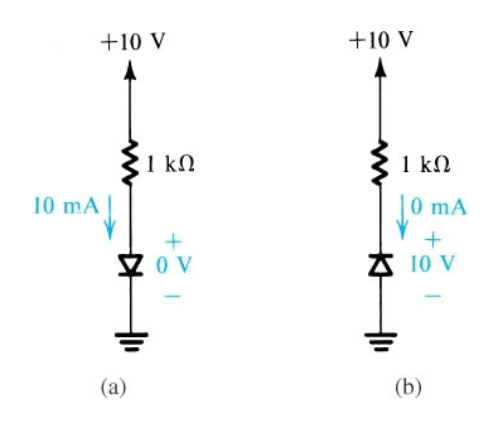
Sample Problem
Calculate the current in the ideal circuits below:
What are the three types of junction diodes?
There are three main types of junction diodes: Light Emitting Diodes (LEDs), Photodiodes, and Solar Cells. LEDs are commonly used in music system displays and railway station information boards, creating vibrant and dynamic lighting effects. Photodiodes (PN junction diodes) are made from a photosensitive semiconductor. They are used to convert light into electrical current, finding applications in devices like light meters and barcode scanners. Solar cells, on the other hand, are designed to convert light energy into electrical energy. Serving as a key component in solar panels for generating electricity. Another important type is the Zener diode, which is used for voltage regulation in electronic circuits.
What is a Pn junction diode?
A p-n junction diode is a fundamental semiconductor device that regulates the flow of electric current within a circuit. It is comprised of a positive (p) side and a negative (n) side, established by introducing impurities into opposite sides of a silicon semiconductor. The symbol representing a p-n junction diode is a triangle pointing towards a line.
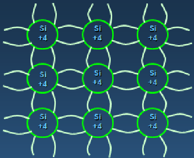
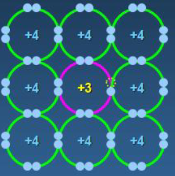
It is made primarily of silicon (Si) or germanium (Ge), both of which are group 4 elements in the periodic table. As a result, they both have 4 valence electrons. In a silicon diode, for example, silicon atoms are arranged in a crystal lattice structure. Each silicon atom has 4 valence electrons, which form covalent bonds with neighboring atoms, creating a stable structure. Each Si atom shares one electron with each of its four closest neighbors so that its valence band will have a full 8 electrons.
N-Type Material
Introducing additional valence electrons into a material like silicon creates an n-type material. These extra electrons are introduced by adding impurities or dopants to the silicon. Group V elements are used as dopants to create an n-type material, with arsenic, antimony, and phosphorus being the most commonly used dopants from Group V.
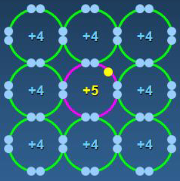
silicon. This extra electron is very mobile.
P-Type Material
The introduction of a dopant from Group III elements creates p-type material. Group III elements have three valence electrons, leaving a deficiency of one electron, which results in the creation of a hole (h+), or a positive charge that can move within the material. Commonly used Group III dopants include aluminum, boron, and gallium.
hole is quite mobile in the same way the extra electron is mobile in an n-type material.
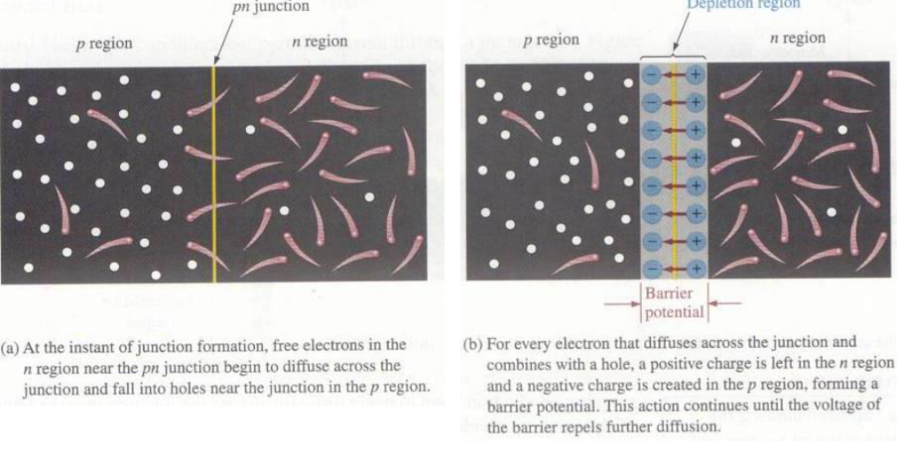
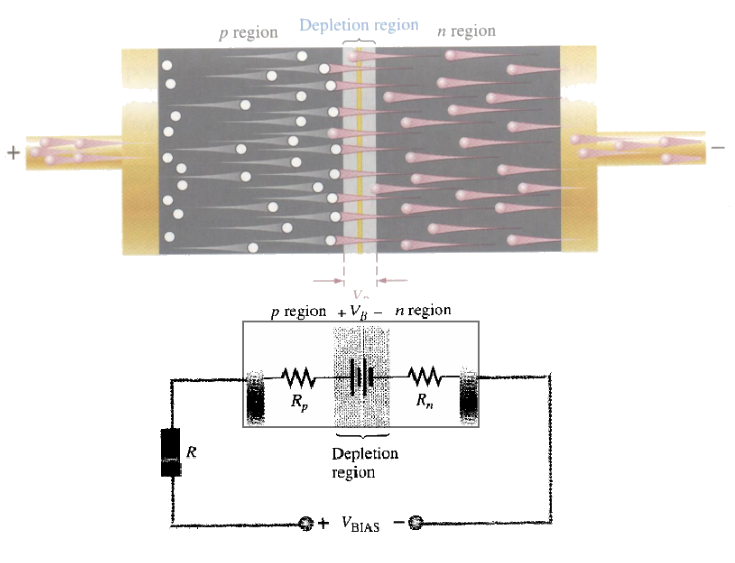
The PN-Junction
The boundary between p-type and n-type material is referred to as a pn-junction. When a voltage is applied across the diode, the electric field pushes the free electrons in the N-type material (which has an excess of electrons) towards the P-type material (which has a deficiency of electrons), and the holes in the P-type material towards the N-type material. This movement of charge carriers creates a region near the junction of the P and N-type materials called the depletion zone. In this depletion zone, there are no free-charge carriers.
Forward Bias:
When the positive terminal of a DC voltage source is connected to the p region and the negative terminal to the n region, it creates a condition that allows current to flow through the pn-junction of a diode.
In normal operation, when the diode is forward-biased (positive voltage applied to the P-type material and negative voltage to the N-type material), the depletion zone shrinks, allowing current to flow across the junction. This occurs because the electric field from the applied voltage overcomes the built-in potential of the diode, which is the potential barrier created by the depletion zone.
Reverse Bias:
When the negative terminal of a DC voltage source is connected to the p region and the positive terminal to the n region, the depletion region widens until its potential difference equals the bias voltage, causing the majority-carrier current to cease.

Conversely, when the diode is reverse-biased (positive voltage applied to the N-region and negative voltage to the P region), the depletion zone widens. Thus preventing current flow across the junction. This is because the applied voltage adds to the built-in potential. Thus making it more difficult for charge carriers to overcome the barrier.
Conclusion
In summary, a diode works by using the properties of semiconductors to control the flow of current in a circuit, allowing current to flow in one direction while blocking it in the other direction. Diodes are versatile components used in a wide range of applications, from converting AC to DC and signal isolation to voltage regulation and light emission in LEDs. Understanding the basic principles of diodes is essential for anyone interested in electronics, as they form the building blocks of many electronic circuits and devices.