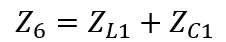
2nd Order RLC Circuit
A 2nd Order RLC Circuit incorporate two energy storage elements. An RLC electrical circuit consisting of a resistor (R), an inductor (L), and a capacitor (C) arranged either in series or in parallel. The circuit’s name originates from the letters used to its constituent the three components. These circuits are described by a second-order differential equation. Typically, the characteristic equation, derived from the governing differential equation, serves as a tool for identifying the natural response of the circuit.
Introduction
This report details the computation of transfer functions for a given 2nd Order RLC Circuit. Although all values within this report are specific to the problem circuit, the general approach used could be applied to any arbitrary second order electrical circuits consisting of the same set of components to determine its transfer function response.
2nd Order RLC Circuit: Problem Statement
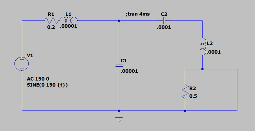
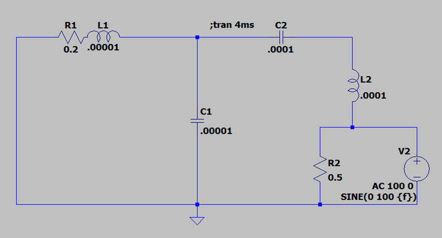
The 2nd Order RLC Circuit seen below in Figure 1 was the premise of this project. The goal of this project was to vary the frequency of the two voltage sources, V1 and V2, over the range of 0 – 1 MHz simultaneously and determine the transfer function with output voltage across the capacitor C1. The given constant properties of each component are also listed below. R1 and R2 represent the resistors, L1 and L2 represent the inductors, and C1 and C2 represent the capacitors in Figure 1.1.
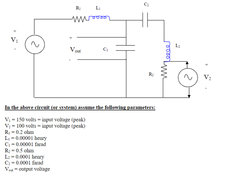
Figure 1.1: Problem Statement / Example of 2nd Order RLC Circuit
The following sections will cover the general methods and techniques used to analyze this circuit. The subsequent section will demonstrate the solutions for the transfer functions between V1 and V2 and Vout.
Method
The system behaves linearly, meaning that all resistances, capacitances, and inductances are invariable. With assumption two, we can assume that superposition applies. The definition for superposition, as defined by A. Hambley, states: “The total response is the sum of the responses to each of the independent sources acting individually.” Applying superposition to this model, we can state:

(1.a)
Since we have assumed superposition, we can treat the left-hand side of the circuit, Response( V1 ), and the right-hand side, Response( V2 ), independently.
Definition of terms in a 2nd Order RLC Circuit
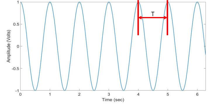
This section will cover the terminology and definitions for sinusoidal voltages, phasor definitions, and complex impedances. To start with sinusoidal voltages, Figure 1.2 below is an example of a sinusoidal voltage with a constant amplitude and frequency. Where “T” in figure 1.2 shows the period of the sine wave.
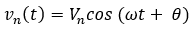
Equation 1.2 for the plot in Figure 1. b is given by the following:
(1.b)
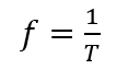
Where V_n is the peak value of the amplitude in Volts, ω is the angular frequency in rad/s, and θ is the phase angle. The angular frequency can be calculated using the following equations, where the frequency, f in Hz, is calculated using the following equations 1.c and 1.d:
(1.c)
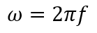
(1.d)
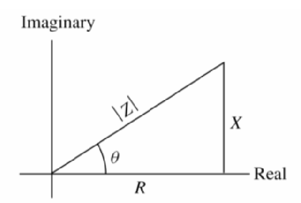
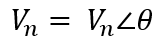
Phasors are used to communicate the voltages and currents as complex number vectors (Hambley pg. 222). This means that the phasor form of the sinusoidal voltage can be seen below in equation 1.e:
(1.e)
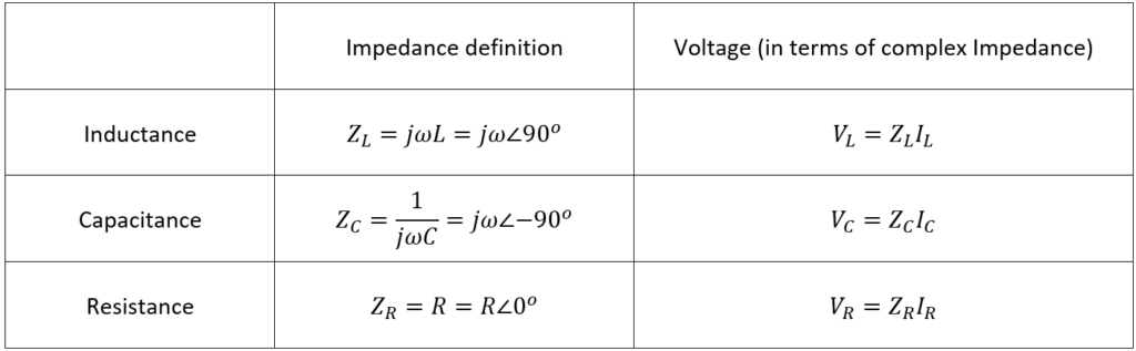
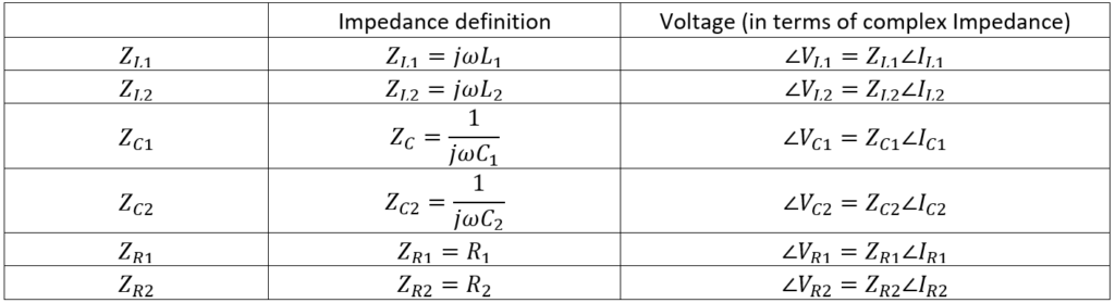
With the sinusoidal voltages and phasors defined, the last term definition to be covered is complex impedances. Impedances are commonly used to simplify circuit analysis because we can apply Kirchoff’s Voltage and Current laws to systems represented by impedances. This circuit contains inductors, capacitors, and resistances. The impedances and resulting voltages are shown in Table 1.1.
2nd Order RLC Circuit: Solution
To begin the analysis, the principle of superposition is assumed. The following circuit diagram in Figure 2.1 below can be represented completely using impedances as shown in Figure 2.2. Note that R2 is crossed out in the diagram because V2 is shorted; all current would pass through the short instead of over the resistance.
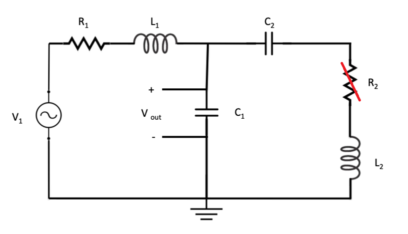
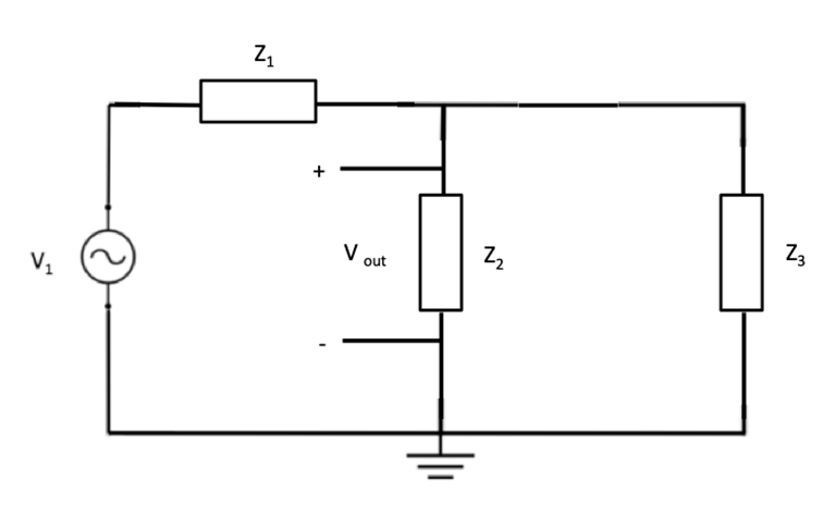
Figure 2.2 uses the impedances delineated in Table 2.1. Note that Phasor notation is being called out with the “∠” symbol for this paper.
Transfer Function between Vout and V1 (Left-Hand Side)
Solution: Solved Theoretically
First, V2 was zeroed out to compute the response of the circuit to V1. The resultant circuit diagram is shown in Figure 2.1. Note that R2 is not present in the diagram because V2 is shorted; all current would pass through the short instead of over the resistance. When the circuit elements are converted into their equivalent complex impedances are shown in Table 2.1, the combination of the elements in series and parallel results in the diagram shown in Figure 2.2. Where the impedances for Z_1, Z_2, and Z_3 are given by the following see equations 2. a, 2.b, and 2. c:
(2.a)
(2.b)
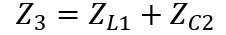
(2.c)
Finally, these complex impedances are summed into a single equivalent impedance for the circuit using equation 2.d, allowing the total current to be determined with Ohm’s Law.
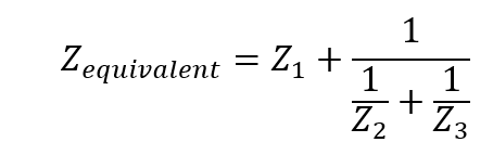
(2.d)
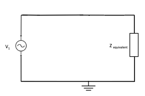
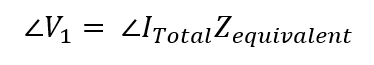
Having thus simplified the circuit, we can solve for ∠I_total, the phasor current within the circuit as we have computed Z_equivalent and were given ∠ V1 see equation 2.e:
(2.e)
Once we have solved for ∠I_Total we must determine the voltage across the capacitor selected as Vout . To do so, we can leverage the current-division principle, which is applied to the simplified circuit. Using this principle, we find ∠I_Z2 using equation 2.f:
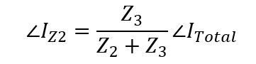
(2.f)
This provides us with the current across Z_2. Using Ohm’s Law, ∠V_C1 can be computed since ∠I_Z2 and Z_2 are known quantities. Since ∠V_C1 is equivalent to ∠ Vout we can construct the transfer function for H1(f) = |Vout,1 (f) / V1 (f)|. The MATLAB code below was used to compute the transfer function H1(f).
Z1 = constR1 + 1i .* w .* constL1;
Z2 = 1 ./ (1i .* w .* constC1);
Z3 = (1 ./ (1i .* w .* constC2)) + 1i .* w .* constL2;
Zeq = Z1 + 1 ./ ((1 ./ Z2)+(1 ./ Z3));
I_t = constV1 ./ Zeq;
I_z2 = (Z3 ./ (Z2 + Z3)) .* I_t;
Vout = I_z2 .* Z2;
H1 = Vout ./ constV1;
H1_mag = abs(H1); %Magnitude for Bode plot
H1_deg = (180/pi).angle(H1); %Phase angle to plot H1_mag_plot = 20log10(H1_mag); %Apply dB conversion for ease of plotting
%--------------------------------------------------------------------------
Equation 2.g is found by combining the circuit equations shown into a general form. Note: this is limited in terms of impedances. This equation could be decomposed easily to a more basic form using the values for each given in Table 2.1 if desired.
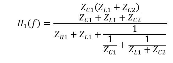
(2.g)
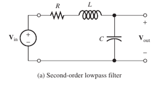
During the development of this analysis, it was noted that the circuit analyzed closely resembles a second-order lowpass filter. The dotted green line in the above plots was computed and plotted alongside the circuit equation-based transfer function. The results very closely agree, being nearly line-on-line over most of the region, providing supporting evidence that the analysis was correct. The theoretical low-pass filter results were found by using formulas found in A. Hambley – Electrical Engineering Principles and Applications, 6th Edition. The left-hand side of the problem circuit is a second-order lowpass filter, see Figure 2.4 below.
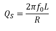
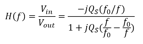
Equations 2.h, 2.i and 2.j below are sourced from the A. Hambley text. Equations I and II yield the filter circuit’s quality factor Q_S and resonant frequency f_0. Both values are readily computed from the given quantities and can then be plugged into equation III. MATLAB is again leveraged to solve for H1(f) for each frequency in the vector, which is much preferred to performing this calculation by hand.
(2.h)
(2.i)
(2.j)
Which can be solved using the following code from MATLAB
%For V1 active - Second-order Lowpass Filter - Calculate fixed values -----
%Source: A. Hambley 6th Ed, Chapter 6, second-order low pass filter
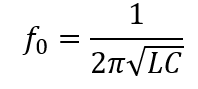
f0 = 1 / (2 * pi * sqrt(constL1 * constC1)); % resonant freq
Qs = (2 * pi * f0 * constL1) / constR1; % quality factor
%--------------------------------------------------------------------------
%Calculate theoretical values for each frequency for V1 active ------------
H1_theory = (-1 * 1i * Qs * (f0 ./f)) ./ (1 + 1i * Qs * (f./f0 - f0./f));
H1_theoryMag = abs(H1_theory); %Magnitude for Bode plot
H1_theoryDeg = (180/pi).angle(H1_theory); %Phase angle to plot H1_theoryMag_Plot = 20log10(H1_theoryMag); % Apply dB conversion for plot
%--------------------------------------------------------------------------
Solution: Solved using LTSpice
The circuit in Figure 2.1 was simulated using LTSpice and correlated to the output of the MATLAB code. The LTSpice model is built as shown in Figure 2.5. This model was used to perform an AC Frequency Sweep analysis within LTSpice for 1 Hz to 1 MHz. The sweep started at 1Hz because 0Hz produces a DC signal which was not valid for the AC simulation.
Graphical Response
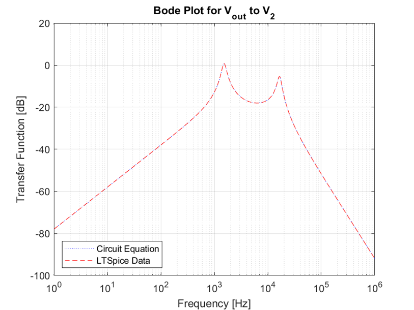
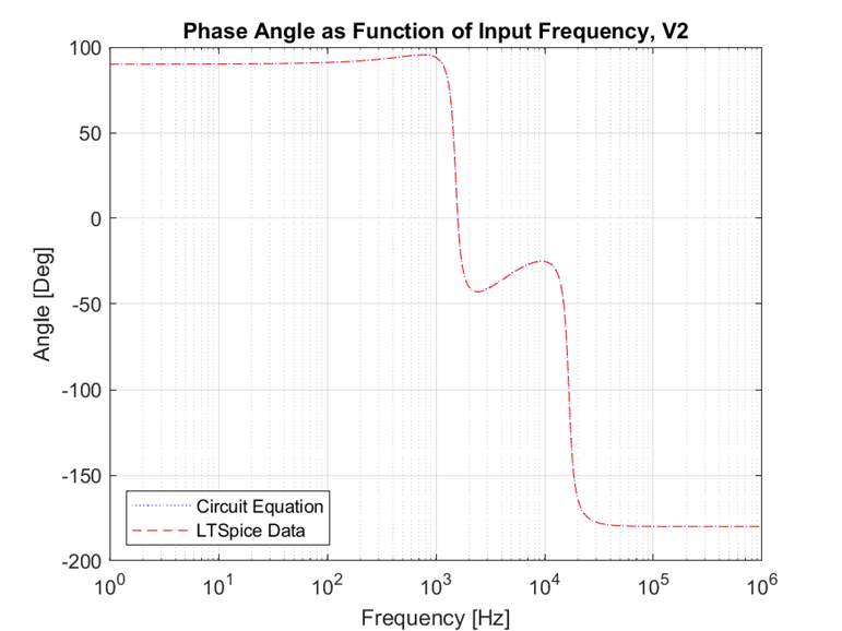
The values for the transfer function were calculated using simulation (LTSpice Model) and theoretically using MATLAB and the method described in section 2.2.1. The goal was to calculate the transfer function and demonstrate the graphical response with a Bode plot, comprised of the magnitude and phase diagram, as shown in Figure 2.6 and Figure 2.7, respectively.
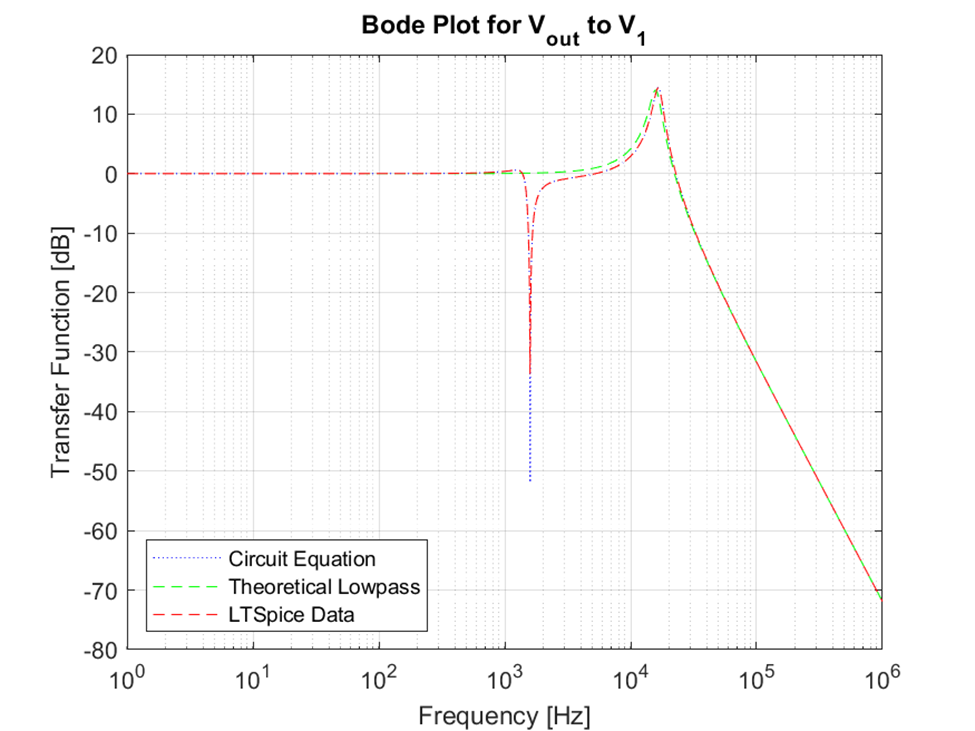
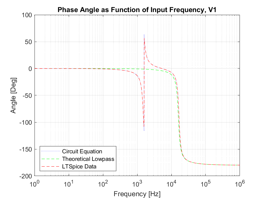
One item to note is the impact of the natural frequency. f_0 for the second-order lowpass filter is 16kHz, which matches up with the transfer function peak in Figure 2.8. If we consider only the additional portion from the second-order lowpass filter, its f_0 is 1.6kHz, aligning with the phase angle inversion and transfer function valley in the above plots.
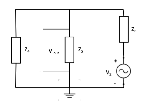
Transfer Function between Vout and V2 (Right-Hand Side)
Solution: Solved theoretically
Following the same process, superposition is now applied to the right-hand side of the problem circuit, assuming only V2 to be active. Additionally, R2 can be eliminated as it is in parallel with an ideal voltage source. The resultant circuit diagram is shown in Figure 2.8. The complex impedances for the elements shown in the figure can be found in Table 2.3.
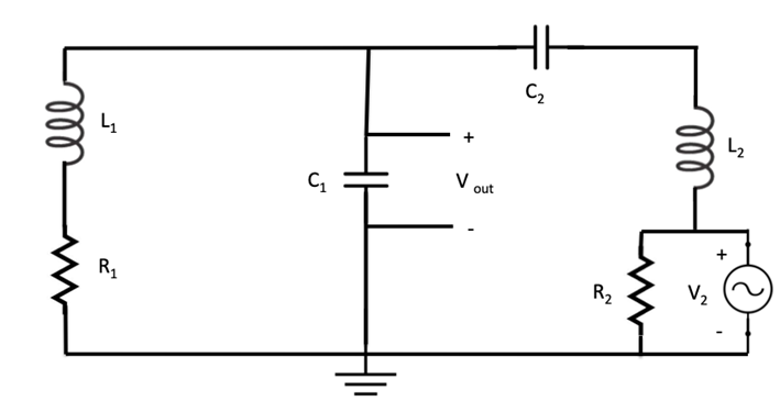
Figure 2.8: Resultant Circuit Diagram (Right-Hand Side)
Further simplifying by summing a series of complex impedances together, the partially simplified circuit is shown in Figure 2.9 with the representative impedances shown below.
(2.k)
(2.l)
(2.m)
%For V1 active - Second-order Lowpass Filter - Calculate fixed values -----
%Source: A. Hambley 6th Ed, Chapter 6, second-order low pass filter
f0 = 1 / (2 * pi * sqrt(constL1 * constC1)); % resonant freq
Qs = (2 * pi * f0 * constL1) / constR1; % quality factor
%--------------------------------------------------------------------------
%Calculate theoretical values for each frequency for V1 active ------------
H1_theory = (-1 * 1i * Qs * (f0 ./f)) ./ (1 + 1i * Qs * (f./f0 - f0./f));
H1_theoryMag = abs(H1_theory); %Magnitude for Bode plot
H1_theoryDeg = (180/pi).angle(H1_theory); %Phase angle to plot H1_theoryMag_Plot = 20log10(H1_theoryMag); % Apply dB conversion for plot
%--------------------------------------------------------------------------
Combining the circuit equations shown into a general form, Equation 2.n is found. Note: this is limited in terms of impedances for each given circuit element, in order to keep the equation manageable. This equation could be decomposed easily to a more basic form using the values for each given in Table 2.1 if desired.
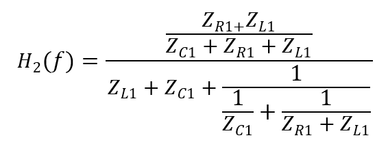
(2.n)
Again, MATLAB is used to solve for the total circuit current at each frequency. This again be used in conjunction with the current division principle to find ∠I_Z5, the phasor current across the element of interest. Ohm’s Law can be applied to find ∠V_C1 which is equivalent to ∠ Vout , which again is simplified to magnitude and phase angle.
Solution: Solved using LTSpice
The provided circuit was again modeled in LTSpice and used to check the output of the MATLAB code. To cross-check, the LTSpice model was used to perform an AC frequency sweep, and the result overlaid on the Bode plots shown in the next section. The LTSpice model layout used for the frequency sweep is as shown in Figure 2.10.
Graphical Response
The transfer functions calculated with MATLAB and LTSpice are displayed for comparison below. Note that there is no discrepancy in the models between these two analysis methods. The bode plot for magnitude is shown in Figure 2.11 and Figure 2.12 shows the phase plot.
The mechanical-analog system
For the final portion of the assignment, an analogous mechanical system was developed using the guiding principles shown in Table 3.1.
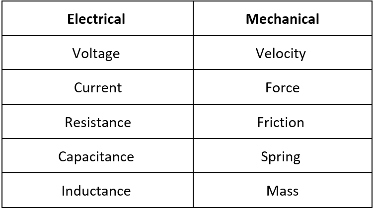
Table 3.1: Electrical-Mechanical Analog
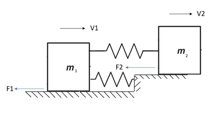
Figure 3.1 below shows the electrical system from Figure 1, translated to a mechanical system analog. Using the values in Table 1, all circuit elements were converted to their analogous mechanical system entities or forces, allowing the above system to be developed. Using the standard cartesian coordinate system, Velocity 1 [V1] and Velocity 2 [V2] are going towards the positive X directions where the Friction 1 [F1] and Friction 2 [F2] are opposing those velocities respectively.
Summary
The circuit in Figure 1.1 was analyzed to determine the theoretical transfer functions for both input voltages. If a very precise understanding of the circuit behavior is needed, the next step would be to perform physical testing and characterization of the circuit. The left-hand side graphed transfer functions for V1 match very well between the various analysis techniques. The theoretical low-pass filter matches the left-hand side solution except for the notch at 1.6kHz which is seen in the LTSpice and circuit equations. The variation is due to the addition of the capacitor and inductor in the given circuit. The right-hand side graphed transfer functions for V2 match very well between the various analysis techniques. Additionally, this analysis made assumptions of ideal components, so a real system would exhibit different behavior due to resistivity and temperature fluctuation.
Works Cited
Hambley, Allan R. Electrical Engineering: Principles and Applications 6th Ed. Upper Saddle River, N.J: Prentice Hall, 2014.
Appendix
Full MATLAB Script Source Code:
%Performs calculations for plot generation for ECE 510 Project #1 ---------
%Assumptions
%   -Superposition is valid for V1 and V2 considered separately
%   -All given circuit components and conductors are ideal
%--------------------------------------------------------------------------
%Setup - Initial commands -------------------------------------------------
clearvars; clc; clf;
%--------------------------------------------------------------------------
%Constants - Given in problem statement -----------------------------------
constV1 = 150; %[Volt] Peak input voltage V1
constV2 = 100; %[Volt] Peak input voltage V2
constR1 = 0.2; %[Ohm]
constL1 = 0.00001; %[Henry]
constC1 = 0.00001; %[Farad]
constR2 = 0.5; %[Ohm]
constL2 = 0.0001; %[Henry]
constC2 = 0.0001; %[Farad]
%--------------------------------------------------------------------------
%For V1 active - Second-order Lowpass Filter - Calculate fixed values -----
%Source: A. Hambley 6th Ed, Chapter 6, second-order low pass filter
f0 = 1 / (2 * pi * sqrt(constL1 * constC1)); % resonant freq
Qs = (2 * pi * f0 * constL1) / constR1; % quality factor
%--------------------------------------------------------------------------
%Set up vectors for frequency [Hz] and [Rad/s] for use in calcs -----------
f = 0:1000000; w = 2*pi*f; %set up frequency range [Hz] and [Rad/s]
%--------------------------------------------------------------------------
%Calculate theoretical values for each frequency for V1 active ------------
H1_theory = (-1 * 1i * Qs * (f0 ./f)) ./ (1 + 1i * Qs * (f./f0 - f0./f));
H1_theoryMag = abs(H1_theory); %Magnitude for Bode plot
H1_theoryDeg = (180/pi).*angle(H1_theory); %Phase angle to plot
H1_theoryMag_Plot = 20*log10(H1_theoryMag); % Apply dB conversion for plot
%--------------------------------------------------------------------------
%Calculate values for each frequency for V1 active - ref circuit diagrams -
Z1 = constR1 + 1i .* w .* constL1;
Z2 = 1 ./ (1i .* w .* constC1);
Z3 = (1 ./ (1i .* w .* constC2)) + 1i .* w .* constL2;
Zeq = Z1 + 1 ./ ((1 ./ Z2)+(1 ./ Z3));
I_t = constV1 ./ Zeq;
I_z2 = (Z3 ./ (Z2 + Z3)) .* I_t;
Vout = I_z2 .* Z2;
H1 = Vout ./ constV1;
H1_mag = abs(H1); %Magnitude for Bode plot
H1_deg = (180/pi).*angle(H1); %Phase angle to plot
H1_mag_plot = 20*log10(H1_mag); %Apply dB conversion for ease of plotting
%--------------------------------------------------------------------------
%Calculate values for each frequency for V2 active - ref circuit diagrams -
Z4 = constR1 + 1i .* w .* constL1;
Z5 = 1 ./ (1i .* w .* constC1);
Z6 = 1i .* w .* constL2 + 1 ./ (1i .* w .* constC2);
Zeq2 = Z6 + 1 ./ ((1./Z5)+(1./Z4));
I_t2 = constV2 ./ Zeq2;
I_z5 = ( Z4 ./ (Z5 + Z4)) .* I_t2;
Vout2 = I_z5 .* Z5;
H2 = Vout2 ./ constV2;
H2_mag = abs(H2); %Magnitude for Bode plot
H2_deg = (180/pi).*angle(H2); %Phase angle to plot
H2_mag_plot = 20*log10(H2_mag); %Convert to dB for plotting
%--------------------------------------------------------------------------
%--------------------------------------------------------------------------
% pull in raw data from LTSpice run using LTspice2Matlab ------------------
% Credit: https://github.com/PeterFeicht/ltspice2matlab
ltspceData1 = LTspice2Matlab('510 group project Source1.raw');
ltspceFreq1 = ltspceData1.freq_vect; %Freq vector for plot
ltspiceH1 = 20*log10(abs(ltspceData1.variable_mat(3,:)./150));
ltspiceTheta1 = (180/pi).*angle(ltspceData1.variable_mat(3,:)./150);
%--------------------------------------------------------------------------
% pull in raw data from LTSpice run using LTspice2Matlab ------------------
% Credit: https://github.com/PeterFeicht/ltspice2matlab
ltspceData2 = LTspice2Matlab('510 group project Source2.raw');
ltspceFreq2 = ltspceData2.freq_vect; %Freq vector for plot
ltspiceH2 = 20*log10(abs(ltspceData2.variable_mat(2,:)./100));
ltspiceTheta2 = (180/pi).*angle(ltspceData2.variable_mat(2,:)./100);
%--------------------------------------------------------------------------
% generate plots for V1  --------------------------------------------------
figure(1);
semilogx(f,H1_mag_plot,':b',f,H1_theoryMag_Plot,'--g', ...
         ltspceFreq1, ltspiceH1, '--r');
title('Bode Plot for V_o_u_t to V_1');
xlabel('Frequency [Hz]'); ylabel('Transfer Function [dB]');
legend('Circuit Equation', 'Theoretical Lowpass', 'LTSpice Data',...
       'Location','southwest'); grid on;
saveas(gcf,'Figure_1.png'); hold off;
figure(2);
semilogx(f, H1_deg,':b', f,H1_theoryDeg, '--g', ...
         ltspceFreq1, ltspiceTheta1, '--r');
hold on; title('Phase Angle as Function of Input Frequency, V1');
xlabel('Frequency [Hz]'); ylabel('Angle [Deg]');
legend('Circuit Equation', 'Theoretical Lowpass', 'LTSpice Data',...
       'Location','southwest'); grid on;
saveas(gcf,'Figure_2.png'); hold off;
%--------------------------------------------------------------------------
% generate plots for V2 ---------------------------------------------------
figure(3);
semilogx(f,H2_mag_plot,':b', ltspceFreq2, ltspiceH2, 'r--');
title('Bode Plot for V_o_u_t to V_2');
xlabel('Frequency [Hz]'); ylabel('Transfer Function [dB]');
legend('Circuit Equation','LTSpice Data', 'Location','southwest'); grid on;
saveas(gcf,'Figure_3.png'); hold off;
figure(4);
semilogx(f, H2_deg,':b', ltspceFreq2,ltspiceTheta2, 'r--');
hold on; title('Phase Angle as Function of Input Frequency, V2');
xlabel('Frequency [Hz]'); ylabel('Angle [Deg]');
legend('Circuit Equation','LTSpice Data', 'Location','southwest'); grid on;
saveas(gcf,'Figure_4.png'); hold off;
%--------------------------------------------------------------------------
Full LTSpice Model ‘.asc’ file
Version 4
SHEET 1 1300 680
WIRE -160 -128 -256 -128
WIRE -16 -128 -80 -128
WIRE 192 -128 64 -128
WIRE 368 -128 192 -128
WIRE 576 -128 432 -128
WIRE 576 -48 576 -128
WIRE -256 32 -256 -128
WIRE 192 48 192 -128
WIRE 576 96 576 32
WIRE 576 96 496 96
WIRE 736 96 576 96
WIRE 496 160 496 96
WIRE 736 160 736 96
WIRE -256 288 -256 112
WIRE 192 288 192 112
WIRE 192 288 -256 288
WIRE 496 288 496 240
WIRE 496 288 192 288
WIRE 736 288 736 240
WIRE 736 288 496 288
WIRE 192 320 192 288
FLAG 192 320 0
SYMBOL res -64 -144 R90
WINDOW 0 0 56 VBottom 2
WINDOW 3 32 56 VTop 2
SYMATTR InstName R1
SYMATTR Value 0.2
SYMBOL cap 176 48 R0
SYMATTR InstName C1
SYMATTR Value .00001
SYMBOL cap 432 -144 R90
WINDOW 0 0 32 VBottom 2
WINDOW 3 32 32 VTop 2
SYMATTR InstName C2
SYMATTR Value .0001
SYMBOL ind -32 -112 R270
WINDOW 0 32 56 VTop 2
WINDOW 3 5 56 VBottom 2
SYMATTR InstName L1
SYMATTR Value .00001
SYMBOL ind 560 -64 R0
SYMATTR InstName L2
SYMATTR Value .0001
SYMBOL voltage -256 16 R0
WINDOW 3 24 152 Left 2
WINDOW 123 24 124 Left 2
WINDOW 39 0 0 Left 0
SYMATTR Value SINE(0 150 {f})
SYMATTR Value2 AC 150 0
SYMATTR InstName V1
SYMBOL voltage 736 144 R0
WINDOW 3 -188 123 Left 2
WINDOW 123 -111 97 Left 2
WINDOW 39 0 0 Left 0
WINDOW 0 -46 10 Left 2
SYMATTR Value SINE(0 100 {f})
SYMATTR Value2 AC 100 0
SYMATTR InstName V2
SYMBOL res 480 144 R0
SYMATTR InstName R2
SYMATTR Value 0.5
TEXT 992 -232 Left 2 !.tran 4ms
TEXT 992 -336 Left 2 !.param f=1000000
TEXT 992 -272 Left 2 !.ac lin 100000 1 1000000